General Description
The RT4533 is a highly integrated LED driver IC capable of driving 10 WLEDs in series. It is composed of a current mode Boost converter integrated with a 36.5V/1.2A power switch. The RT4533 supports a wide input voltage range from 2.5V to 5.5V, and runs at a fixed frequency of 1.1MHz. The LED current is set via an external resistor and the feedback voltage is regulated to 200mV. For brightness dimming, the RT4533 supports PWM dimming which determines the feedback reference voltage.
Performance Sepcification Summary
Summary of the RT4533GJ6 Evaluation Board performance specificiaiton is provided in Table 1. The ambient temperature is 25°C.
Table 1. RT4533 Evaluation Board Performance Specification Summary
|
Specification
|
Test Conditions
|
Min
|
Typ
|
Max
|
Unit
|
|
Input Voltage Range
|
|
2.5
|
--
|
5.5
|
V
|
|
Output Current
|
|
0
|
--
|
20
|
mA
|
|
Default Output Voltage
|
|
--
|
36.5
|
--
|
V
|
|
Operation Frequency
|
|
--
|
1.1
|
--
|
MHz
|
Power-up Procedure
Suggestion Required Equipments
- RT45336GJ6 Evaluation Board
- DC power supply capable of at least 6V and 2A
- Function Generator
- Oscilloscope
Proper measurement equipment setup and follow the procedure below.
1. Apply 3.6V nominal input power supply (2.5V < VIN < 5.5V) to the VIN and GND terminals.
2. The EN voltage is pulled to logic high by internal circuit to enable operation. Drive EN high (> 1.4V) to enable operation or low (< 0.4V) to disable operation. Pull EN pin to High pin that make EN voltage equal to VIN.
3. There is a 3-pin header JP5 “EN” for enable control. To use a jumper at “H” option to tie EN test pin to input power VIN for enabling the device. Inversely, to use a jumper at “L” option to tie EN test pin and ground GND for disabling the device. The JP5 is also the PWM control pin.
4. The ILED setting supports PWM dimming as below.
Output ILED Setting
1. PWM Brightness Dimming
The EN pin is used for the control input for both PWM dimming mode and digital dimming mode. Shutdown delay when the EN voltage is logic low for more than specific time, the driver will be shut down.
2. OCP
The driver provides cycle-by-cycle current limit function to control the current on power switch. The boost switch turns off when the inductor current reaches this current threshold and it remains off until the beginning of the next switching cycle. This protects the RT4533 and external component under overload conditions.
3. OVP
The Over Voltage Protection is detected by a resistor divider circuit from VOUT. Once VOUT goes over the OVP voltage, LX pin stops switching and the power N-MOSFET will be turned off. Then, the VOUT will be discharged by external resistor. OVP will be released until EN goes from Lo to Hi again.
4. OTP
As the die temperature is higher than 160°C, the chip also will enter protection mode. The power MOSFET will be turned off during protection mode to prevent abnormal operation. The device is released from shutdown automatically when the junction temperature decreases by 15°C.
Detailed Description of Hardware
Headers Description and Placement
Carefully inspect all the components used in the EVB according to the following Bill of Materials table, and then make sure all the components are undamaged and correctly installed. If there is any missing or damaged component, which may occur during transportation, please contact our distributors or e-mail us at evb_service@richtek.com.
Test Points
The EVB is provided with the test points and pin names listed in the table below.
|
Test Point/
Pin Name
|
Signal Name
|
Description
|
|
LX
|
Switch Node
|
This is the switching node of the IC. Connect the switched side of the inductor to LX.
|
|
GND
|
Ground
|
Ground.
|
|
FB
|
Feedback Voltage Input
|
Connect the sense resistor from FB to GND.
|
|
EN
|
Enable Control Input
|
Control pin of the boost converter. It is a multifunctional pin which can be used for enable control and PWM dimming.
|
|
VOUT
|
Output Voltage
|
The output supply pin for the IC. It is used to sense the output voltage for open LED protection.
|
|
BAT
|
Supply Voltage Input
|
The input supply pin for the IC. Support 2.5V to 5.5V input voltage.
|
Bill of Materials
|
Reference
|
Count
|
Part Number
|
Value
|
Description
|
Package
|
Manufacturer
|
|
U1
|
1
|
RT4533GJ6
|
RT4533GJ6
|
DC-DC Converter
|
TSOT-23-6
|
RICHTEK
|
|
L1
|
1
|
NR4018T220M
|
22µH
|
Inductor
|
L-SH4018
|
TAIYO YUDEN
|
|
C2
|
1
|
GRM188R61C225KE15D
|
2.2µF
|
Capacitor Ceramic,
16V/X5R
|
C-0603
|
MURATA
|
|
C5
|
1
|
UMK212ABJ105KD-T
|
1µF
|
Capacitor Ceramic, 50V/X5R
|
C-0805
|
TAIYO YUDEN
|
|
D1
|
1
|
SR26
|
|
Schottky Diode
|
D-1206
|
PANJIT
|
|
R6
|
1
|
WR06X10R0FTL
|
10
|
Resistor, 1%
|
R-0603
|
WALSIN
|
|
D9, D13
|
2
|
WR06X000 PTL
|
0
|
Resistor, Jumper
|
R-0603
|
WALSIN
|
|
D2, D3, D4, D5, D6, D7, D8, D10, D11, D12
|
10
|
LNL-190UW-4H
|
|
WLED
|
D-0603
|
LighTop
|
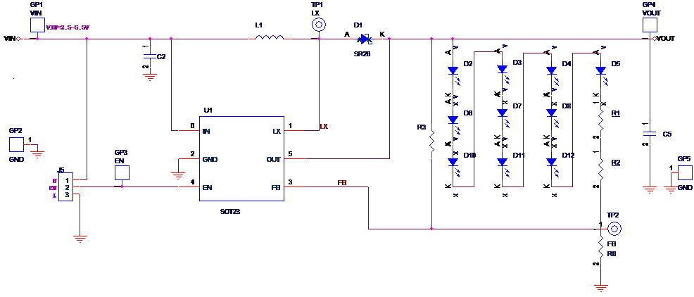
Typical Applications
EVB Schematic Diagram
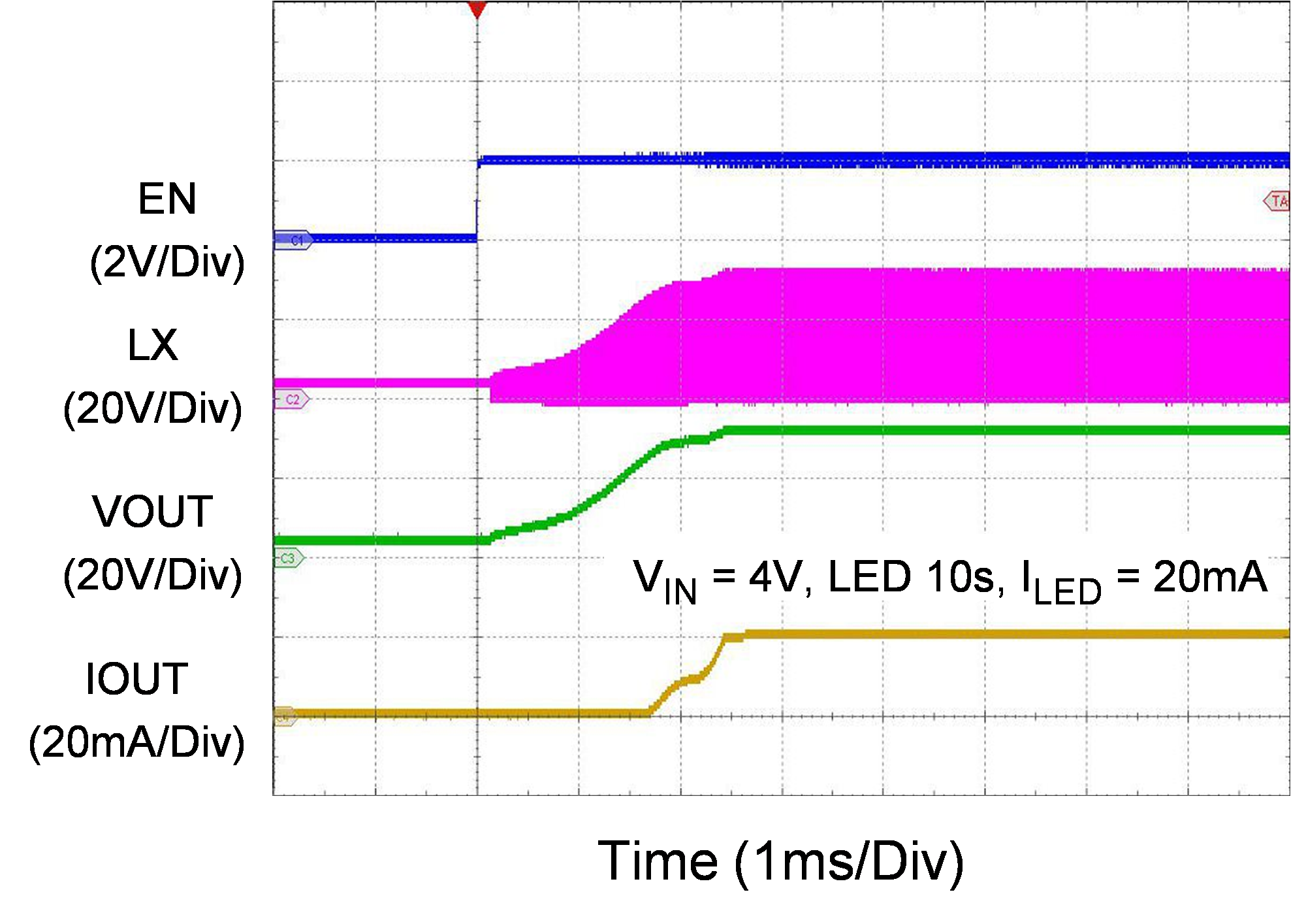
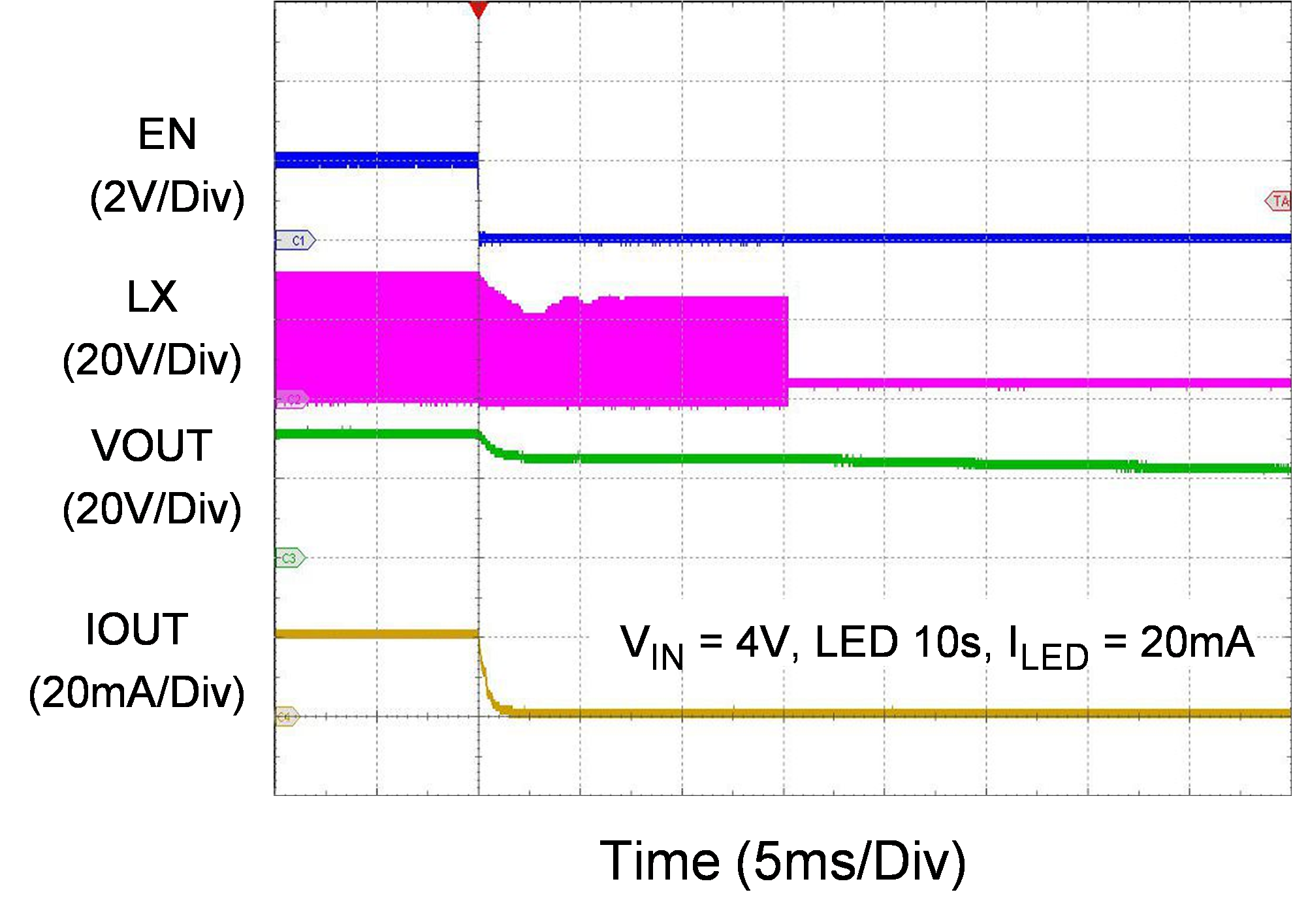
Measure Result
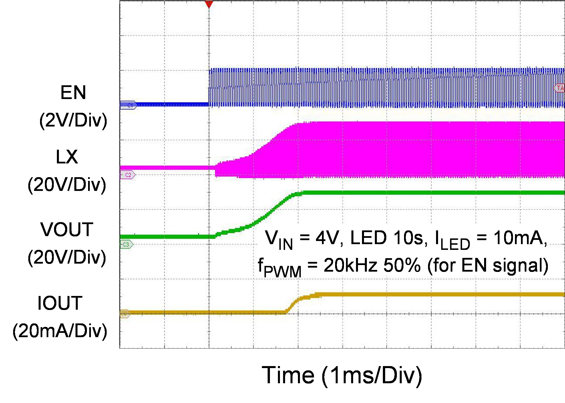
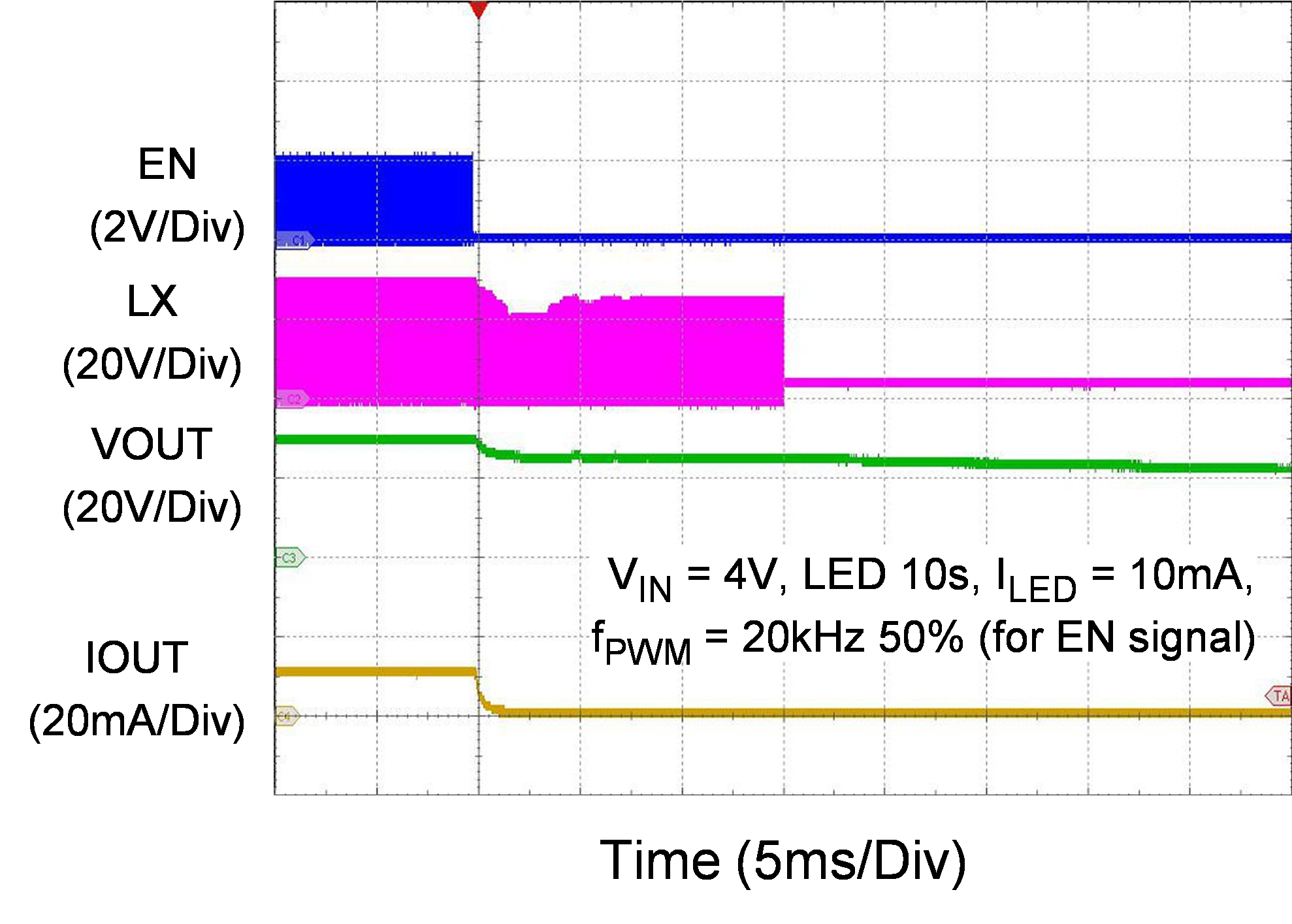
|
Power-On from EN
|
Power-Off from EN
|
|
|
|
|
Power-On and PWM Dimming from EN
|
Power-Off and PWM Dimming from EN
|
|
|
|
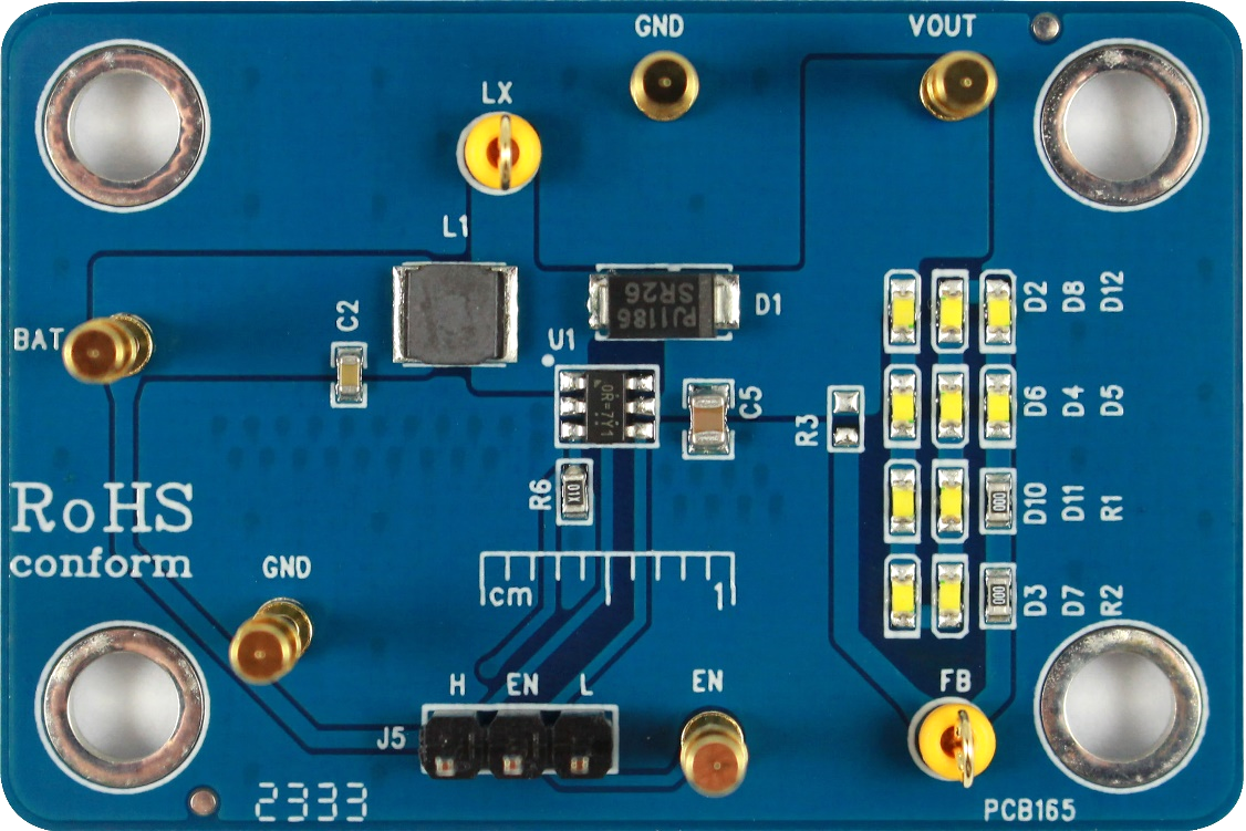
Evaluation Board Layout
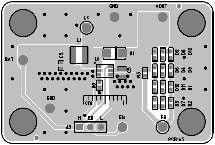
Figure 1. Top View (1st layer)
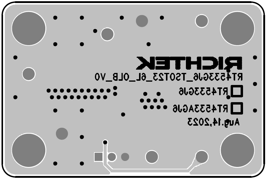
Figure 2. Bottom View (2nd Layer)